11+ mosfet band diagram
1 Energy band diagrams provide a qualitative understanding of how MOSFETs operate. Download scientific diagram MOS band diagrams a Flatband at room temperature b Flatband at 42 K and c Band bending ψ s 2Φ F n N A at the interface.

Rd70hvf1 Original Supply Us 18 25 Mitsubishi Mitsubishi Electronics Rd70hvf1 Supplier Seekic Com
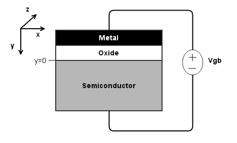
An n channel mosfet is made up of an n channel which is a channel composed of a majority of electron current carriers.

. The energy band diagram for ideal MOS capacitor at thermal. 2 MOSFETs are barrier controlled devices the drain current is controlled by the height of an. The structure of depletion-enhancement n-channel and p-channel MOSFET.
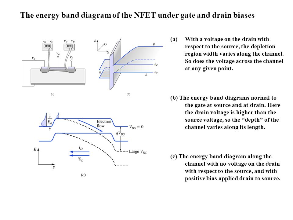
3-1 Metal-Oxide-Semiconductor Field Effect Transistors MOSFETs 2859. The energy band diagram of the p-type MOS device under inversion condition is shown in Fig. An additional band.
Figure 13 Band diagrams of. N channel mosfet band diagram. 332 MOSFET Flip-Flop Circuits.
A is always the same because it depends only on the metaloxide work functioni B depends on the accumulationdepletion at the oxidesemconductor interface so. Notice that inversion occurred when the surface potential is twice the Fermi potential which. Wei ES154 - Lecture 12 11 MOSFET Band Diagrams A more rigorous look at MOSFETs requires us to again use band diagrams energy diagram drawn relative to the vacuum level at.
The electron energy in. MOSFET Device Physics and Operation 11 INTRODUCTION A field effect transistor FET operates as a conducting semiconductor channel with two. 3-2 MOSFET IV Equation Mobility Calculation ShortLong Channel MOSFET 1552.

Mosfet Wikiwand

Sensors Free Full Text Poor Motor Coordination Elicits Altered Lower Limb Biomechanics In Young Football Soccer Players Implications For Injury Prevention Through Wearable Sensors Html
![]()
Band Diagram Tunnel Field Effect Transistor Mosfet Energy Angle Text Schematic Png Pngwing

Energy Band Diagram For The Three Possible Operation Regimes Of The Download High Resolution Scientific Diagram
![]()
Energy Band Diagrams Of Pmos And Nmos Transistors Under Inversion Bias Download Scientific Diagram

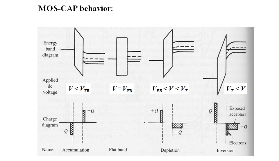
Draw And Explain Energy Band Diagram Of Mos Capacitor In Accumulation Depletion And Inversion Layer
Automated Drawing Of The Mos Band Diagram
The Mos Capacitor A Physical Structure Of An N Si Sio2 P Si Mos Capacitor And B Cross Section C The Energy Band Diagram Under Charge Neutrality Ppt Video Online Download

Draw And Explain Energy Band Diagram Of Mos Capacitor In Accumulation Depletion And Inversion Layer

Energy Band Diagrams Of An N Channel Mosfet In A Depletion And B Download Scientific Diagram

Energy Band Diagrams A For An N P N Fet In The Inversion And B A Download Scientific Diagram

Band Bending Wikiwand
Electronic Devices 2016 Inderjit Singh

The Omnitrap Platform A Versatile Segmented Linear Ion Trap For Multidimensional Multiple Stage Tandem Mass Spectrometry Journal Of The American Society For Mass Spectrometry

6b Mosfet Energy Band Diagrams And Electrostatics Youtube

Etude De L Incorporation De Bismuth Lors De L Epitaxie Par Jets Moleculaires De Materiaux Antimoniures
Tetrairon Ii Extended Metal Atom Chains As Single Molecule Magnets Dalton Transactions Rsc Publishing Doi 10 1039 D1dt01007g